Field-Programmable Gate Arrays (FPGAs) have become a pivotal element in modern digital design, offering flexibility, speed, and customization that traditional fixed-function hardware cannot match. However, they are notoriously difficult to debug and for this reason it is important to use Continuous Integration (CI) to ensure your devices are regularly tested.
In this post, we’ll dive into the synthesis and hardware testing processes for AMD FPGAs, following a practical tutorial that utilizes BeetleboxCI, a powerful CI tool. This tutorial outlines how to create and run a hardware testbench, synthesize a full adder design, and test it on an FPGA using the Integrated Logic Analyzer (ILA) IP core.
If you prefer your tutorials in video format, you can also check it out here:
You can also find the detailed verison of this tutorial here.
You can find all the source code for this tutorial here.
Understanding the FPGA Design Flow
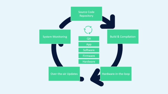
The FPGA design process is multi-faceted, involving several critical steps that transform high-level design concepts into hardware implementations. Here’s an overview of the fundamental stages:
- Design Entry: The initial stage where the design’s architecture is captured using hardware description languages (HDLs) such as VHDL or Verilog.
- Simulation: Pre-synthesis simulation is performed to verify the design’s functionality, ensuring that the logic behaves as intended before moving to hardware. We have already written about how to automate simultion here.
- Synthesis: Converts HDL code into a gate-level netlist, mapping the design to FPGA primitives.
- Implementation: The synthesized netlist is placed and routed onto the FPGA’s physical architecture, meeting timing and area constraints.
- Testing and Debugging: Involves programming the FPGA and using tools like the ILA to capture real-time data for performance analysis and debugging.
The Role of Continuous Integration in FPGA Development
Continuous Integration (CI) is increasingly becoming a staple in FPGA development. Traditionally associated with software, CI brings automation and collaboration benefits to hardware design:
- Automated Builds and Tests: CI tools automate the synthesis and testing processes, enabling consistent builds and rapid validation of code changes.
- Collaboration: CI facilitates team collaboration through shared repositories and standardized workflows, minimizing integration issues.
- Early Error Detection: By integrating automated testing early in the design process, CI helps identify and rectify issues before they escalate.
Setting Up the FPGA Design Environment
Before diving into synthesis and testing, it’s essential to set up a robust development environment. Here’s a concise guide to preparing your tools and project setup:
- Install Vivado Design Suite: Ensure you have the AMD Vivado Design Suite installed, as it provides all the necessary tools for design, simulation, synthesis, and testing.
- Configure Project Settings: Set up your Vivado project with the correct constraints and HDL files. Linking your project with a version control system like Git is crucial for collaboration.
- Get BeetleboxCI for free here: Integrate your project with BeetleboxCI, enabling automated builds, simulations, and tests.
- Have a Git provider linked to BeetleboxCI. Make sure to have an account with a Git repository provider such as GitHub, BitBucket or Azure DevOps. BeetleboxCI will need access to your provider and you can find the documentation for that here.
- Have your FPGA ready. For this tutorial we will be using a Digilent Arty A7 100-t, but feel free to use your own board. You may need to vary certain parameters for your board.
Creating IP to test
For this tutorial, you will be creating a simple full adder in VHDL. Of course feel free to swap in your own designs instead. Makes sure to add this as a design source yo your Vivado project. Here is the code for the full adder below:
library IEEE;
use IEEE.STD_LOGIC_1164.ALL;

entity adder is
  Port ( A : in STD_LOGIC;
    B : in STD_LOGIC;
    CIN: in STD_LOGIC;
    S: out STD_LOGIC;
    COUT: out STD_LOGIC);
end adder;

architecture Behavioral of adder is
begin
    S <= A xor B xor CIN;
    COUT <= (A and B) or (CIN and (A xor B));

end Behavioral;
Creating and Running a Hardware Testbench
To validate a design on an FPGA, you must first create a hardware testbench. Here’s a step-by-step overview of the process:
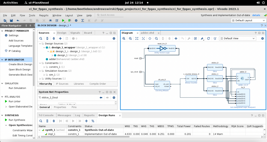
- Block Diagram Creation:
- Open Vivado and navigate to the Flow Navigator.
- Select Create Block Design under IP Integrator and confirm the setup.
- Add Full Adder Module:
- Locate your full adder module under Design Sources.
- Right-click and select Add Module to Block Diagram.
- Integrate Clock Source:
- Add the
Clocking WizardIP to provide a clock source. - Use Connection Automation to automatically configure clock and reset pins.
- Add the
- Include a Counter:
- Add a 3-bit
Binary CounterIP to drive inputs for the full adder. - Re-customize the IP to ensure correct output width and connect to the clock.
- Add a 3-bit
- Slice and Connect Inputs:
- Add three
SliceIPs to separate the counter outputs. - Connect each slice to respective inputs (
A,B,Cin) of the full adder.
- Add three
- Attach the ILA Core:
- Add the
ILAIP and customize it for monitoring signals. - Connect the ILA probes to outputs and inputs of the full adder.
- Add the
- Validate and Generate Design:
- Validate the block diagram to ensure correctness.
- Generate the block design and create an HDL wrapper for synthesis.
Running the Hardware Testbench
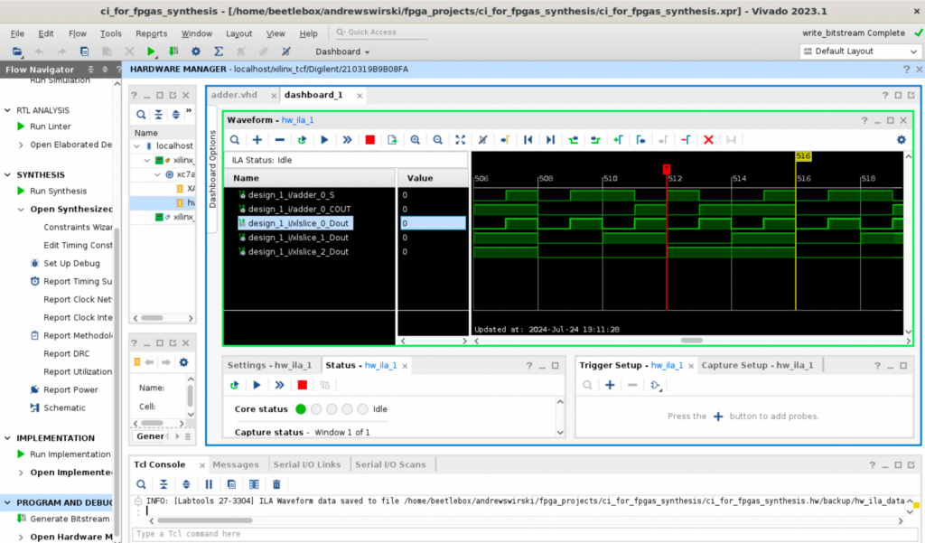
Once your design is synthesized and implemented, it’s time to program the FPGA and capture results using the ILA:
- Program the FPGA:
- Open the Hardware Manager in Vivado.
- Connect to your FPGA device and program it with the generated bitstream.
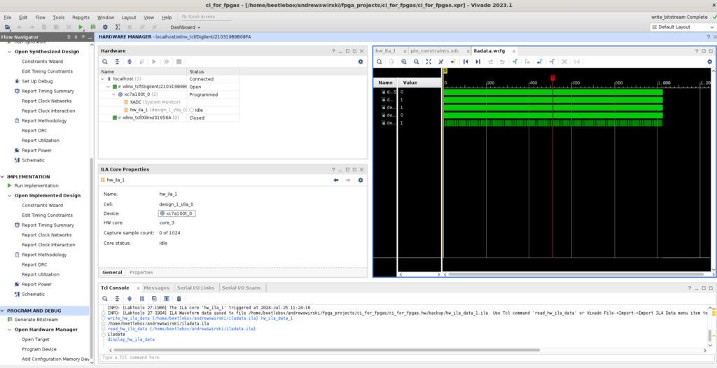
- Capture ILA Data:
- Use the ILA to capture real-time waveforms of your design running on the FPGA.
- Analyze the captured data to verify functionality and make sure that matches the expected behaviour of a full adder.
Automating the Hardware Testbench with BeetleboxCI
To streamline testing, automate the hardware testbench using BeetleboxCI:
- Update Git Repository:
- Add the generated files for synthesis and programming to your Git repo.
- Update the
.gitignorefile to manage the files correctly.
# Blocklist files/folders in same directory as the .gitignore file
/*

# Includelist some files
!.gitignore
!README.md

# Include xpr and srcs
!ci_for_fpgas.srcs/
!ci_for_fpgas.srcs/*
!ci_for_fpgas.xpr

# Include gen files
!ci_for_fpgas.gen/
!ci_for_fpgas.gen/*

!tcl_scripts/
!tcl_scripts/*

!.bbx/
!.bbx/*- Create Constraints File:
- Define pin constraints for your FPGA board to ensure correct mapping. This may vary according to your board.
set_property PACKAGE_PIN E3 [get_ports sys_clock]
set_property IOSTANDARD LVCMOS33 [get_ports sys_clock]
set_property PACKAGE_PIN C2 [get_ports reset]
set_property IOSTANDARD LVCMOS33 [get_ports reset]- Write TCL Scripts:
run_synthesis.tcl: Automates synthesis, implementation, and bitstream generation. You will need to vary this file to use your own project name instead ofci_for_fpgas.
program_device_trigger_ila.tcl: Automates device programming and ILA triggering. You will need to vary this file to use your own project name instead ofci_for_fpgasand also change it to target your device instead ofxc7a100t_0
run_synthesis.tcl
open_project ci_for_fpgas.xpr
update_compile_order -fileset sources_1
reset_run impl_1 -prev_step
launch_runs impl_1 -to_step write_bitstream -jobs 4
program_device_trigger_ila.tcl
open_hw_manager
connect_hw_server -allow_non_jtag
open_hw_target
set_property PROBES.FILE {./ci_for_fpgas.runs/impl_1/design_1_wrapper.ltx} [get_hw_devices xc7a100t_0]
set_property FULL_PROBES.FILE {./ci_for_fpgas.runs/impl_1/design_1_wrapper.ltx} [get_hw_devices xc7a100t_0]
set_property PROGRAM.FILE {./ci_for_fpgas.runs/impl_1/design_1_wrapper.bit} [get_hw_devices xc7a100t_0]
program_hw_devices [get_hw_devices xc7a100t_0]
refresh_hw_device [lindex [get_hw_devices xc7a100t_0] 0]
run_hw_ila [get_hw_ilas -of_objects [get_hw_devices xc7a100t_0] -filter {CELL_NAME=~"design_1_i/ila_0"}]
wait_on_hw_ila [get_hw_ilas -of_objects [get_hw_devices xc7a100t_0] -filter {CELL_NAME=~"design_1_i/ila_0"}]
display_hw_ila_data [upload_hw_ila_data [get_hw_ilas -of_objects [get_hw_devices xc7a100t_0] -filter {CELL_NAME=~"design_1_i/ila_0"}]]
write_hw_ila_data {./iladata.ila} hw_ila_data_1- Create a Configuration File:
- Create a
config.yamlfile to define new jobs and artifacts for synthesis and testing. - Configure resource specifications to ensure adequate memory for synthesis.
- Make sure to change
ci_for_fpgasto the name of your project and make sure to point towards your installation directory for Vivado.
- Create a
# Example config file to use as a starting point.
# Please visit https://docs.beetleboxci.com/docs/config/configuration-yaml for guidance on setting up your configuration file.

# Define a runner that will be used to run a job
runners:
 ubuntu-runner:
  image: public.ecr.aws/y2s4f3y9/ubuntu-generic

# Define a job to be performed during a workflow
jobs:
 run-sim-syn-job:
  # Specify the runner used to perform this job
  runner: ubuntu-runner
  resource_spec: large
  output:
   artifact:
    - ci_for_fpgas.sim/
    - ci_for_fpgas.hw/
    - ci_for_fpgas.runs/
    - ci_for_fpgas.cache/
    - iladata.ila
  volumes:
    - mount:
        name: volume1
        path: < The installation directory of Xilinx tools, by default this is /tools/Xilinx>

  # Define one or more steps to execute commands as part of the job
  steps:
   - run:
      name: Initalise vivado environment
      command: |
        apt-get update
        apt-get install locales
        locale
        locale-gen "en_US.UTF-8"
        update-locale LANG=en_US.UTF-8
   - run:
      name: Run Simulation
      command: |
        cd < The installation directory of Vivado, by default this is /tools/Xilinx/Vivado/2023.1/>
        source settings64.sh
        cd $HOME
        ls
        vivado -mode batch -source tcl_scripts/run_sim.tcl  | tee simulation_output.txt
   - run:
      name: Parse simulation for errors
      command: |
        # Path to the file to be checked
        FILE_PATH="./simulation_output.txt"
        # Check if the file exists
        if [[ ! -f "$FILE_PATH" ]]; then
         echo "File does not exist: $FILE_PATH"
          exit 1
        fi
        # Search for the phrase "Error: Assertion violation" in the file
        if grep -q "Error: Assertion violation" "$FILE_PATH"; then
          echo "Error: Assertion violation found in file."
          exit 1
        else
          echo "No assertion violations found. Passing."
          exit 0
        fi
   - run:
      name: Run Bitstream Generation
      command: |
        cd /tools/Xilinx/Vivado/2023.1/
        source settings64.sh
        cd $HOME
        vivado -mode batch -source tcl_scripts/run_gen_bitstream.tcl  | tee bit_stream_gen_output.txt
   - run:
      name: Program Device and Trigger ILA
      command: |
        cd /tools/Xilinx/Vivado/2023.1/
        source settings64.sh
        cd $HOME
        vivado -mode batch -source tcl_scripts/program_device_trigger_ila.tcl  | tee program_device_trigger_ila.txt

# Define a workflow to orchestrate a job
workflows:
 run-sim-syn-workflow:
  jobs:
   - run-sim-syn-job
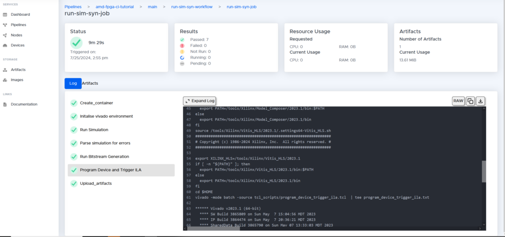
- Run CI Pipeline:
- Execute the CI pipeline in BeetleboxCI to automate synthesis, programming, and testing.
- Review artifacts and ILA data to validate your design.
Real-World Applications and Benefits
By integrating BeetleboxCI into your FPGA workflow, you unlock numerous benefits:
- Enhanced Efficiency: Automating repetitive tasks allows engineers to focus on innovation and design optimization.
- Improved Collaboration: Shared repositories and standardized workflows enable seamless teamwork and integration.
- Faster Iterations: Rapid testing and feedback loops accelerate development cycles, reducing time-to-market.
Conclusion
Congratulations on completing this tutorial on synthesizing and testing AMD FPGAs using BeetleboxCI! By embracing CI for FPGA development, you enhance your workflow with automation, consistency, and collaboration. As the field of digital design continues to evolve, mastering these tools and techniques will empower you to tackle increasingly complex projects with confidence and efficiency.